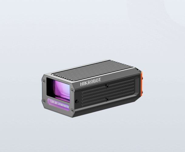
SC6500P Wafer ID Reader | NIR light
Add Zip code to check availability
Select Quantity
Features
Marketplace Benefits
Warranty & Return Policy
Long Description
MV-SC6500P-AI-WID-IBN
SC6500P Series Wafer ID Reader – Mono, Combined IR Light Source
The MV-SC6500P-AI-WID-IBN is a high-precision Wafer ID Reader developed specifically for semiconductor manufacturing environments requiring stable, repeatable, and ultra-high-accuracy wafer identification. It integrates advanced imaging, intelligent illumination, deep learning algorithms, and industrial-grade hardware into a compact, reliable platform ideal for wafer tracking, automation systems, and semiconductor process control.
Powered by the SC6500P architecture and equipped with the Vision Master Platform + SCClient, this device supports a wide range of wafer ID marking types, including SEMI-standard OCR characters, Data Matrix codes, 1D barcodes, and QR codes. Its Near-Infrared (NIR) combined LED light source significantly enhances contrast on challenging wafer surfaces, such as highly polished wafers, etched marks, laser-engraved IDs, and low-contrast characters.
Advanced Features & Benefits
1. High-Accuracy Wafer Identification
The device includes robust OCR and code-reading algorithms compatible with SEMI standards. It reliably reads:
SEMI OCR wafer characters
DataMatrix codes
QR codes
1D barcodes
Deep learning modules improve performance on difficult wafer marks, partial characters, reflective surfaces, and non-uniform illumination conditions.
2. Intelligent NIR Combined Lighting
The integrated Near-Infrared LED illumination offers superior performance compared to visible light in semiconductor environments.
Key advantages:
Enhances visibility of engraved, etched, or low-contrast wafer IDs
Reduces glare and reflections from smooth or mirror-finished wafers
Supports both bright-field and dark-field lighting methods
Fully configurable illumination intensity through software
This makes the device ideal for advanced wafer lines, including 200 mm and 300 mm wafer processing.
3. High-Speed Image Acquisition
The reader includes a CMOS global shutter sensor optimized for fast and stable imaging:
Resolution: 1408 × 576
Pixel size: 3.45 µm
Max frame rate: 120 fps
Exposure time: 25 µs to 1 s
Pixel format: Mono 8
The high-speed capture is ideal for integration into automated wafer handling arms, wafer sorting machines, FOUP/SMIF load ports, and inspection modules where throughput is critical.
4. Auto-Focus Optical System
Equipped with an M12 mount lens and intelligent auto-focus, the reader automatically adjusts to the optimal focus position to maintain imaging clarity across:
Different wafer thicknesses
Slight deviations in wafer position
Adjustable installation heights (40–50 mm recommended)
This minimizes mechanical adjustments and simplifies integration into OEM semiconductor tools.
5. Strong Processing Platform
The SC6500P hardware platform provides:
8 GB memory
64 GB storage
Support for deep learning inference
Real-time data processing and communication
Fast algorithm execution for high-throughput wafer manufacturing lines
6. Industrial-Grade Interfaces
A wide range of industrial protocols ensures easy integration with semiconductor equipment:
TCP / UDP
MODBUS
Serial Port
PROFINET
EtherNet/IP
FINS
MC
FTP
The Gigabit Ethernet interface ensures fast data transfer and low-latency communication with host systems.
7. Compact, Durable Mechanical Design
Built for reliability in semiconductor facilities:
Ingress protection: IP40
Dimensions: 127 × 69 × 49 mm
Weight: 829 g
Humidity tolerance: 20–95% RH (non-condensing)
Working temperature: 0–40°C
The rugged design ensures stable performance under cleanroom conditions and continuous operation in automated semiconductor equipment.
8. Efficient Power & I/O
Power supply: 24 VDC
Power consumption:
Typical: 11.5 W
Maximum: 18 W
Digital I/O:
Non-isolated input × 1
Non-isolated output × 1
RS-232 × 1
Typical Applications
Wafer ID reading for 200 mm / 300 mm wafers
Wafer sorting and classification stations
FOUP/SMIF load port identification
Track & trace across semiconductor production lines
Lithography, etching, CMP, deposition, and inspection tools
Semiconductor MES data binding and automation equipment
Why Choose MV-SC6500P-AI-WID-IBN?
Superior ID readability using NIR illumination
Faster, more reliable performance on difficult wafer surfaces
High-speed sensor for automation lines
Deep learning-enhanced accuracy
Compact industrial design
Flexible deployment with auto-focus
Seamless connectivity with major industrial protocols