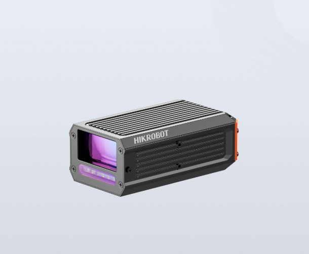
SC6500P Wafer ID Reader | Red LED
Add Zip code to check availability
Select Quantity
Features
Marketplace Benefits
Warranty & Return Policy
Long Description
MV-SC6500P-AI-WID-RBN – SC6500P Wafer ID Reader (Mono, Combined Red Light Source)
The MV-SC6500P-AI-WID-RBN is a specialized Wafer ID Reader designed for semiconductor manufacturing environments. Built on the powerful SC6500P platform with integrated deep learning capabilities, it delivers fast, accurate, and stable identification of SEMI OCR characters, DataMatrix codes, barcodes, and QR codes used on semiconductor wafers.
With its intelligent lighting design, auto-focus M12 lens, and high-speed global-shutter CMOS sensor, this device ensures reliable reading performance across various wafer ID marking styles and surface conditions.
Key Features
High-Performance Reading Capabilities
Supports:
SEMI OCR wafer characters
DataMatrix codes
QR codes
1D barcodes
Built-in Platforms: Vision Master Platform (with deep learning module) + SCClient
Imaging Specifications
Sensor: CMOS, global shutter
Resolution: 1408 × 576
Sensor Size: 1/3.4"
Pixel Size: 3.45 µm × 3.45 µm
Max Frame Rate: 120 fps
Gain: 0–37 dB
Exposure: 25 µs to 1 s
Format: Mono 8
Advanced Lighting System
Integrated Red LED (RGB supported through bar light)
Lighting Modes: Bright field + Dark field
Illumination Intensity: Adjustable via software
Optics & Installation
Lens Mount: M12
Focus: Auto-focus
Recommended Installation Height: 40–50 mm
Field of View: 38 mm × 15 mm
Depth of Field: ± 5 mm
Connectivity & I/O
Data Interface: Gigabit Ethernet (1000 Mbps)
Digital I/O (6-pin P7):
Non-isolated input × 1
Non-isolated output × 1
RS-232 × 1
Platform Specs
Memory: 8 GB
Storage: 64 GB
Electrical
Power Supply: 24 VDC
Power Consumption:
Typical: 11.5 W
Maximum: 18 W
Mechanical & Environmental
Dimensions: 127 × 69 × 49 mm
Weight: 829 g
Protection Rating: IP40
Operating Temperature: 0°C to 40°C
Storage Temperature: –30°C to 70°C
Humidity: 20%–95% RH (non-condensing)
Certifications: CE, KC
Ideal Applications
Semiconductor wafer ID reading
Wafer tracking & traceability systems
Cleanroom inspection environments
Automated wafer handling equipment